
Page 79 - husk_nvidia_-2_n13p-gl
P. 79
D C B A Rev Rev Rev -2 -2 -2 103 103 103
Wistron Corporation Wistron Corporation Wistron Corporation of of of
1 21F, 88, Sec.1, Hsin Tai Wu Rd., Hsichih, 21F, 88, Sec.1, Hsin Tai Wu Rd., Hsichih, 21F, 88, Sec.1, Hsin Tai Wu Rd., Hsichih, Taipei Hsien 221, Taiwan, R.O.C. Taipei Hsien 221, Taiwan, R.O.C. Taipei Hsien 221, Taiwan, R.O.C. 79 79 79 Sheet Sheet Sheet 1
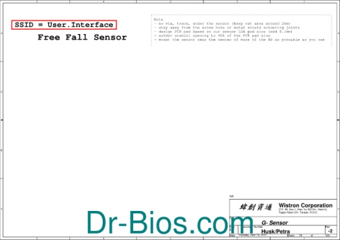
- stay away from the screw hole or metal shield soldering joints
- design PCB pad based on our sensor LGA pad size (add 0.1mm)
- no via, trace, under the sensor (keep out area around 2mm)
G- Sensor G- Sensor G- Sensor Husk/Petra Husk/Petra Husk/Petra
- solder stencil opening to 90% of the PCB pad size
Document Number Document Number Document Number Thursday, April 19, 2012 Thursday, April 19, 2012 Thursday, April 19, 2012
2 - mount the sensor near the center of mass of the NB as possible as you can 2
IVB IVB IVB Title Title Title Size Size Size A4 A4 A4 Date: Date: Date:
3 Dr-Bios.com 3
Note
4 Free Fall Sensor 4
5 SSID = User.Interface 5
D C B A