Page 28 - R2017-REC-ECE-UG Syllabus
P. 28
Department of ECE, REC


                    3.  Cunningham,  W.P.  Cooper,  T.H.  Gorhani,  ‘Environmental  Encyclopedia’,  JaicoPubl.,  House,
                       Mumbai, 2001.
                                                                              rd
                    4.  Rajagopalan.R,  ‘Environmental  studies-  From  Crisis  to  Cure’,3   edition,  Oxford  University  press,
                       2015.


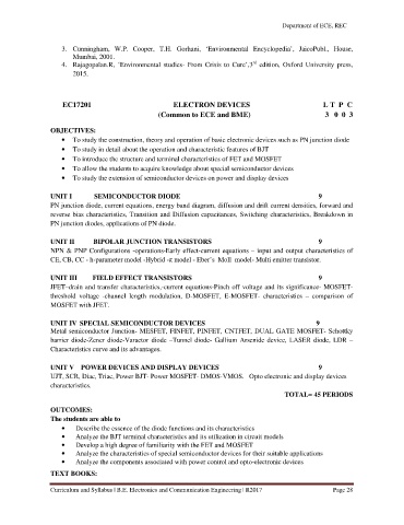
                    EC17201                           ELECTRON DEVICES                                L T  P  C
                                                 (Common to ECE and BME)                                        3   0  0  3

                OBJECTIVES:
                    •  To study the construction, theory and operation of basic electronic devices such as PN junction diode
                    •  To study in detail about the operation and characteristic features of BJT
                    •  To introduce the structure and terminal characteristics of FET and MOSFET
                    •  To allow the students to acquire knowledge about special semiconductor devices
                    •  To study the extension of semiconductor devices on power and display devices

                UNIT I             SEMICONDUCTOR DIODE                                                9
                PN junction diode, current equations, energy band diagram, diffusion and drift current densities, forward and
                reverse bias characteristics, Transition and Diffusion capacitances, Switching characteristics, Breakdown in
                PN junction diodes, applications of PN diode.

                UNIT II           BIPOLAR JUNCTION TRANSISTORS                                       9
                NPN & PNP Configurations -operations-Early effect-current equations – input and output characteristics of
                CE, CB, CC - h-parameter model -Hybrid -π model - Eber’s  Moll  model- Multi emitter transistor.

                UNIT III         FIELD EFFECT TRANSISTORS                                                   9
                JFET–drain and transfer characteristics,-current equations-Pinch off voltage and its significance- MOSFET-
                threshold  voltage  -channel  length  modulation,  D-MOSFET,  E-MOSFET-  characteristics  –  comparison  of
                MOSFET with JFET.

                UNIT IV  SPECIAL SEMICONDUCTOR DEVICES                                                                 9
                Metal semiconductor Junction- MESFET, FINFET, PINFET, CNTFET, DUAL GATE MOSFET- Schottky
                barrier diode-Zener diode-Varactor diode –Tunnel diode- Gallium Arsenide device,  LASER diode,  LDR  –
                Characteristics curve and its advantages.

                UNIT V    POWER DEVICES AND DISPLAY DEVICES                                             9
                UJT, SCR, Diac, Triac, Power BJT- Power MOSFET- DMOS-VMOS.   Opto electronic and display devices
                characteristics.
                                                                                       TOTAL= 45 PERIODS

                OUTCOMES:
                The students are able to
                    •   Describe the essence of the diode functions and its characteristics
                    •   Analyze the BJT terminal characteristics and its utilization in circuit models
                    •   Develop a high degree of familiarity with the FET and MOSFET
                    •   Analyze the characteristics of special semiconductor devices for their suitable applications
                    •   Analyze the components associated with power control and opto-electronic devices
                TEXT BOOKS:

                Curriculum and Syllabus | B.E. Electronics and Communication Engineering | R2017      Page 28

