
Page 44 - Digital Electronics by harish
P. 44
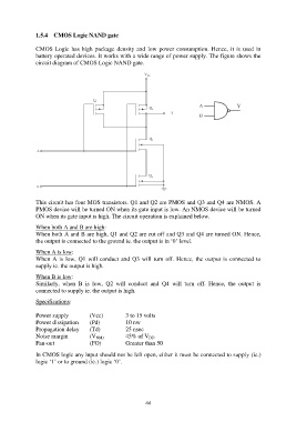
1.5.4  CMOS Logic NAND gate

               CMOS  Logic  has  high  package  density  and  low  power  consumption.  Hence,  it  is  used  in
               battery operated devices. It works with a wide range of power supply. The figure shows the
               circuit diagram of CMOS Logic NAND gate.


               This circuit has four MOS transistors. Q1 and Q2 are PMOS and Q3 and Q4 are NMOS. A
               PMOS device will be turned ON when its gate input is low. An NMOS device will be turned
               ON when its gate input is high. The circuit operation is explained below.

               When both A and B are high:
               When both A and B are high, Q1 and Q2 are cut off and Q3 and Q4 are turned ON. Hence,
               the output is connected to the ground ie. the output is in „0‟ level.

               When A is low:
               When A is  low, Q1 will conduct  and Q3 will turn off. Hence, the output  is  connected to
               supply ie. the output is high.

               When B is low:
               Similarly,  when  B  is  low,  Q2  will  conduct  and  Q4  will  turn  off.  Hence,  the  output  is
               connected to supply ie. the output is high.

               Specifications:

               Power supply          (Vcc)         3 to 15 volts
               Power dissipation     (Pd)          10 nw
               Propagation delay     (Td)          25 nsec
               Noise margin          (V NM)        45% of V DD
               Fan-out               (FO)          Greater than 50

               In CMOS logic any input should not be left open, either it must be connected to supply (ie.)
               logic „1‟ or to ground (ie.) logic „0‟.


                                                           44