Page 81 - REC :: B.E. EEE CURRICULUM & SYLLABUS - R2017
P. 81
Dept of EEE, REC
REFERENCES:
1. Philips, Ravindran and Solberg, “Operations Research”, John Wiley, 2002.
2. Ronald L.Rardin, “Optimization in Operation Research” Pearson Education Pvt. Ltd. New Delhi,
2005.
3. http://www2.pitt.edu/~jrclass/or/or-intro.html
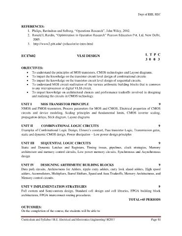
EC17602 VLSI DESIGN L T P C
3 0 0 3
OBJECTIVES:
To understand the principles of MOS transistors, CMOS technologies and Layout diagrams.
To impart the knowledge on the transistor circuit level design of combinational circuits
To impart the knowledge on the transistor circuit level design of sequential circuits.
To understand MOS circuit realization of the various arithmetic building blocks that is common
to any microprocessor or digital VLSI circuit.
To impart knowledge on architectural choices and performance tradeoffs involved in designing
and realizing the circuits in CMOS technology.
UNIT I MOS TRANSISTOR PRINCIPLE 9
NMOS and PMOS transistors, Process parameters for MOS and CMOS, Electrical properties of CMOS
circuits and device modeling, Scaling principles and fundamental limits, CMOS inverter scaling,
propagation delays, Stick diagram, Layout diagrams
UNIT II COMBINATIONAL LOGIC CIRCUITS 9
Examples of Combinational Logic Design, Elmore’s constant, Pass transistor Logic, Transmission gates,
static and dynamic CMOS design, Power dissipation – Low power design principles
UNIT III SEQUENTIAL LOGIC CIRCUITS 9
Static and Dynamic Latches and Registers, Timing issues, pipelines, clock strategies, Memory
architecture and memory control circuits, Low power memory circuits, Synchronous and Asynchronous
design
UNIT IV DESIGNING ARITHMETIC BUILDING BLOCKS 9
Data path circuits, Architectures for Adders, ripple carry adders, carry look ahead adders, High speed
adders, Accumulators, Multipliers, Barrel Shifters, Speed and Area Tradeoffs, Memory Architectures, and
Memory control circuits.
UNIT V IMPLEMENTATION STRATEGIES 9
Full custom and Semi-custom design, Standard cell design and cell libraries, FPGA building block
architectures, FPGA interconnect routing procedures.
TOTAL=45 PERIODS
OUTCOMES:
On the completion of the course, the students will be able to
Curriculum and Syllabus | B.E. Electrical and Electronics Engineering | R2017 Page 81

