
Page 3 - husk_nvidia_-2_n13p-gl
P. 3
4 3 2 1 Rev Rev Rev -2 -2 -2 103 103 103
Wistron Corporation Wistron Corporation Wistron Corporation 21F, 88, Sec.1, Hsin Tai Wu Rd., Hsichih, 21F, 88, Sec.1, Hsin Tai Wu Rd., Hsichih, 21F, 88, Sec.1, Hsin Tai Wu Rd., Hsichih, of of of 3 3 3
E Default Value 1 0 11 1 Taipei Hsien 221, Taiwan, R.O.C. Taipei Hsien 221, Taiwan, R.O.C. Taipei Hsien 221, Taiwan, R.O.C. Table of Content Table of Content Table of Content Husk/Petra Husk/Petra Husk/Petra Sheet Sheet Sheet E
Huron River Schematic Checklist Rev.0_7 ON for supporting Deep Sleep states IVB IVB IVB PCH_SMBDATA/PCH_SMBCLK PCH_SMBDATA/PCH_SMBCLK PCH_SMBDATA/PCH_SMBCLK Title Title Title PCH_SMBDATA/PCH_SMBCLK PCH_SMBDATA/PCH_SMBCLK PCH_SMBDATA/PCH_SMBCLK Document Number Document Number Document Number Size Size Size A3 A3 A3 Thursday, April 19, 2012 Thursday, April 19, 2012 Thursday, April 19, 2012 Date: Date: Date:
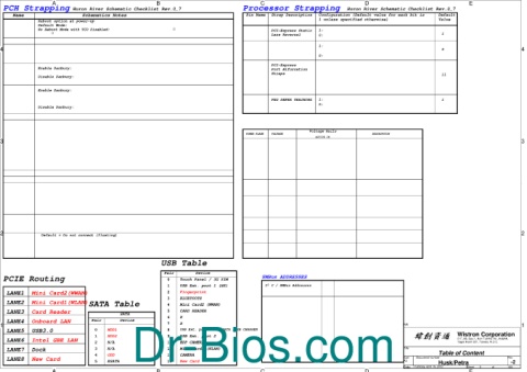
D Configuration (Default value for each bit is 1 unless specified otherwise) Normal Operation. Lane Numbers Reversed 15 -> 0, 14 -> 1, ... Disabled - No Physical Display Port attached to Embedded DisplayPort. Enabled - An external Display Port device is connectd to the EMBEDDED display Port 11 : x16 - Device 1 functions 1 and 2 disabled 10 : x8, x8 - Device 1 function 1 enabled ; function 2 disabled 01 : Reserved - (Device 1 function 1 disabled ; function 2 e
Processor Strapping Strap Description 1: PCI-Express Static Lane Reversal 0: 1: 0: PCI-Express Port Bifurcation Straps enabled PEG DEFER TRAINING 0: Voltage Rails VOLTAGE ACTIVE IN 0.95 - 0.85V 0.35V to 1.5V S0 0.4 to 1.25V S3 6V-14.1V 6V-14.1V All S states WOL_EN DSW, Sx G3, Sx SMBus ADDRESSES I C / SMBus Addresses Ref Des
C Pin Name CFG[2] CFG[4] CFG[6:5] CFG[7] POWER PLANE 5V 5V_S0 3.3V 3D3V_S0 1.8V 1D8V_S0 1.5V 1D5V_S0 1.05V 1D05V_VTT 0D85V_S0 0.75V 0D75V_S0 VCC_CORE VCC_GFXCORE 1.8V 1D8V_VGA_S0 3.3V 3D3V_VGA_S0 1V 1V_VGA_S0 5V 5V_USBX_S3 1.5V 1D5V_S3 0.75V DDR_VREF_S3 BT+ DCBATOUT 5V 5V_S5 5V 5V_AUX_S5 3.3V 3D3V_S5 3.3V 3D3V_AUX_S5 3.3V 3D3V_LAN_S5 3.3V 3D3V_AUX_KBC 3.3V 3D3V_AUX_S5 2 Device EC SMBus 1 Battery CHARGER EC SMBus 2 PCH eDP PCH SMB
USB Table Device Touch Panel / 3G SIM USB Ext. port 1 (HS) Fingerprint BLUETOOTH Mini Card2 (WWAN) CARD READER X X USB Ext. port 4 / E-SATA /USB CHARGER USB Ext. port 2 EDP CAMERA Mini Card1 (WLAN) CAMERA New Card
Huron River Schematic Checklist Rev.0_7 Schematics Notes Connect to Vcc3_3 with 8.2-kΩ GNT[3:0]# functionality is not available on Mobile. Pull-up resistors are not required on these signals. If pull-ups are used, they should be tied to the Vcc3_3power rail. Connect to Vcc3_3 with 8.2-k? weak pull-up resistor. Left floating, no pull-down required. Enable Danbury: Connect to +NVRAM_VCCQ with 8.2-kohm weak pull-up resistor [CRB has it
B Pair 0 1 2 3 4 5 6 7 8 9 10 11 12 13 B
PCH Strapping GNT3#/GPIO55 GNT2#/GPIO53 GNT1#/GPIO51 HAD_DOCK_EN# PCIE Routing USB3.0 Dock
A Reboot option at power-up Internal weak Pull-down. Default Mode: No Reboot Mode with TCO Disabled: - 10-kΩ weak pull-up resistor. Weak internal pull-up. Leave as "No Connect". Mobile: Used as GPIO only Enable Danbury: Disable Danbury: Disable Danbury: strapping functions. suite with confidentiality Note : This is an un-muxed signal. Sampled at rising edge of RSMRST#. enabled. Default = Do not connect (floating) circuits for analog rails. Mi
INIT3_3V#
Name
SPKR
4 SPI_MOSI NV_ALE NC_CLE /GPIO[33] 3 HDA_SDO HDA_SYNC GPIO15 GPIO8 2 GPIO27 LANE1 LANE2 LANE3 LANE4 1 LANE5 LANE6 LANE7 LANE8