
Page 128 - Digital Electronics by harish
P. 128
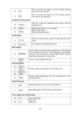
This  is  an active low signal.  It  will be 0 during memory
                      32                    read and I/O read operation.


                                                This  is  an active low signal.  It  will be 0 during memory
                      31                    write and I/O write operation.


                   Peripheral initiated signals
                                                This  pin  is  used  for  interfacing  slow  devices  with  the
                      35      READY             microprocessor.

                      39      HOLD              DMA (Direct Memory Access) signals:
                                                HOLD (hold request)
                      38      HLDA              HLDA (hold acknowledge)


                   Clock signals

                                                Used  for  connecting  the  crystal  for  generating  the  clock
                     1, 2     X 1, X 2          signal.


                      37      CLK OUT           Clock signal for the peripheral devices.

                   Reset signals

                                            Used to apply reset signal to the microprocessor. When this pin
                                            goes low, the microprocessor is reset and begins executing the
                      36         instruction  from  the  memory  location  0000.  All  the  registers
                                            inside the microprocessor is reset to zero.

                              RESET         Used to reset the peripheral devices.
                       3
                              OUT
                   Interrupt signals

                       6      TRAP
                       7      RST 7.5       Interrupt request input signals to the microprocessor.
                       8      RST 6.5
                       9      RST 5.5
                      10      INTR
                                            Interrupt  Acknowledgesignal  from  the  microprocessor  to  the
                      11            peripheral devices.

                   Serial I/O signals


                       5      SID           Serial Input Data. Used to receive serial data bits.

                       4      SOD           Serial Output Data. Used to transmit serial data bits.


                   Power supply and Ground signals

                      40      V CC          Power supply pins.
                                            +5V to V CC
                      20      V             GND to V SS
                                SS


                                                           128