
Page 127 - Digital Electronics by harish
P. 127
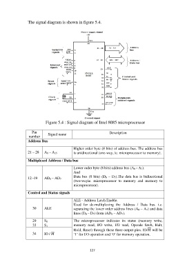
The signal diagram is shown in figure 5.4.


                              Figure 5.4 : Signal diagram of Intel 8085 microprocessor

                      Pin                                              Description
                    number      Signal name
                   Address Bus

                                                Higher order byte (8 bits) of address bus. The address bus
                   21 – 28    A 8 – A 15        is unidirectional (one-way, ie. microprocessor to memory).


                   Multiplexed Address / Data bus
                                                Lower order byte (8 bits) address bus (A 0 - A 7).
                                                And

                   12 -19     AD 0 – AD 7       Data  bus  (8  bits)  (D 0  –  D 7).The  data  bus  is  bidirectional
                                                (two-wayie.  microprocessor  to  memory  and  memory  to
                                                microprocessor).
                   Control and Status signals


                                                ALE - Address Latch Enable.
                                                Used  for  de-multiplexing  the  Address  /  Data  bus.  i.e.
                      30      ALE               separating the lower order address lines (A 0 – A 7) and data
                                                lines (D 0 – D 7) from (AD 0 – AD 7).

                      29      S 0               The  microprocessor  indicates  its  status  (memory  write,
                      33      S 1               memory  read,  I/O  write,  I/O  read,  Opcode  fetch,  Halt,
                                                Hold, Reset) through these three output pins. IO/ will be
                      34      IO /            „1‟ for I/O operation and „0‟ for memory operation.


                                                           127