
Page 155 - Digital Electronics by harish
P. 155
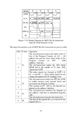
Figure  5.14 Timing Diagram for MOV Rd, Rs instruction
                                           (Opcode Fetch Machine Cycle)

               The steps for machine cycle of MOV Rd, Rs instruction are given in table.

                         S.No  T state  Operation
                                            The microprocessor places the higher order 8-
                                            bits  of  the  Program  Counter  on  A15  –  A8
                           1.               address bus and the lower order 8-bits of the
                                            Program      Counter      on    AD7      –     AD0
                                            address  / data bus.
                                 T1         The  microprocessor  makes  the  ALE  signal
                           2.               HIGH  and  at  the  middle  of  T1  state,  ALE
                                            signal goes LOW.
                                            The status signals are changed as IO/ =  0,
                           3.               S1 =1 and S0 = 1. These status signals do not
                                            change throughout the OF machine cycle.

                                            The microprocessor makes the  line LOW
                           4.               to  enable  memory  read  (opcode  fetch)  and
                                 T2         increments the Program Counter.
                                            The contents on D7 – D0 (i.e. the Opcode) are
                           5.
                                            placed on the address / data bus.
                                            The  microprocessor  transfers  the  Opcode  on
                           6.               the address / data bus to Instruction  Register
                                 T3
                                            (IR).
                           7.               The microprocessor decodes the instruction.
                                            The data in the register Rs (r ) is moved to the
                           8.    T4                                         2
                                            register Rd (r ).
                                                           1


                                                           155