
Page 151 - Digital Electronics by harish
P. 151
The microprocessor makes the line
4. LOW to enable memory read and increments
T the Program Counter.
2
The contents on D7 – D0 (i.e. the data) are
5.
placed on the address / data bus.
The data loaded on the address / data bus is
6. moved to the microprocessor.
T
3
7. The microprocessor makes the line
HIGH to disable the memory read operation.
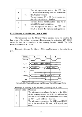
5.3.1.3Memory Write Machine Cycle of 8085
Microprocessor uses the Memory Write machine cycle for sending the
data in one of the registers to memory. For example, the instruction STA 5000H
writes the data in accumulator to the memory location 5000H. The MW
machine cycle takes 3 T-states.
The timing diagram for Memory Write machine cycle is shown in figure
5.12.
Figure 5.12 : Timing Diagram for Memory Write Machine Cycle
The steps in Memory Write machine cycle are given in table.
S.No T State Operation
The microprocessor places the higher order 8-bits
of the memory address on A15 – A8 address bus
1.
and the lower order 8-bits of the memory address
T on AD7 – AD0 address / data bus.
1
The microprocessor makes the ALE signal HIGH
2. and at the middle of T1 state, ALE signal goes
LOW.
151