
Page 154 - Digital Electronics by harish
P. 154
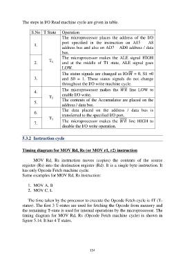
The steps in I/O Read machine cycle are given in table.

                     S.No  T State       Operation
                                         The  microprocessor  places  the  address  of  the  I/O
                                         port  specified  in  the  instruction  on  A15  –  A8
                       1.
                                         address bus and also on AD7 – AD0 address / data
                                         bus.
                                         The  microprocessor  makes  the  ALE  signal  HIGH
                                 T
                       2.         1      and  at  the  middle  of  T1  state,  ALE  signal  goes
                                         LOW.

                                         The status signals are changed as IO/ = 0, S1 =0
                       3.                and  S0  =  1.  These  status  signals  do  not  change

                                         throughout the I/O write machine cycle.
                                         The  microprocessor  makes  the    line  LOW  to
                       4.
                                 T       enable I/O write.
                                  2
                       5.                The contents of the Accumulator are placed on the
                                         address / data bus.
                                         The  data  placed  on  the  address  /  data  bus  is
                       6.                transferred to the specified I/O port.
                                 T
                                  3
                       7.                The  microprocessor  makes  the    line  HIGH  to
                                         disable the I/O write operation.

               5.3.2  Instruction cycle


               Timing diagram for MOV Rd, Rs (or MOV r1, r2) instruction

                       MOV  Rd,  Rs  instruction  moves  (copies)  the  contents  of  the  source
               register (Rs) into the destination register (Rd). It is a single byte instruction. It
               has only Opcode Fetch machine cycle.
               Some examples for MOV Rd, Rs instruction:

                   1.  MOV A, B
                   2.  MOV C, L

                   The time taken by the processor to execute the Opcode Fetch cycle is 4T (T-

               states). The first 3 T-states are used for fetching the Opcode from memory and
               the remaining T-state is used for internal operations by the microprocessor. The
               timing diagram  for  MOV  Rd, Rs  (Opcode  Fetch  machine cycle) is shown  in
               figure 5.14. It has 4 T states.


                                                           154