Page 149 - Digital Electronics by harish
P. 149

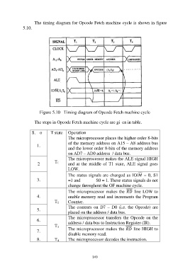
The timing diagram for Opcode Fetch machine cycle is shown in figure
               5.10.


                          Figure 5.10 : Timing diagram of Opcode Fetch machine cycle


                       The steps in Opcode Fetch machine cycle are given in table.

                     S. No       T state  Operation
                                            The microprocessor places the higher order 8-bits
                                            of the memory address on A15 – A8 address bus
                        1.
                                            and the lower order 8-bits of the memory address
                                            on AD7 – AD0 address  / data bus.
                                            The microprocessor makes the ALE signal HIGH
                                   T
                         2           1      and  at  the  middle  of  T1  state,  ALE  signal  goes
                                            LOW.

                                            The status signals are changed as IO/ = 0, S1
                        3.                  =1 and              S0 = 1. These status signals do not

                                            change throughout the OF machine cycle.
                                            The microprocessor makes the  line LOW to
                        4.                  enable memory read and increments the Program
                                   T        Counter.
                                     2
                                            The  contents  on  D7  –  D0  (i.e.  the  Opcode)  are
                        5.
                                            placed on the address / data bus.
                                            The  microprocessor transfers  the  Opcode  on  the
                        6.                  address / data bus to Instruction Register (IR).
                                   T
                                     3
                        7.                  The microprocessor makes the  line HIGH to
                                            disable memory read.

                        8.         T        The microprocessor decodes the instruction.
                                     4


                                                           149
   144   145   146   147   148   149   150   151   152   153   154