
Page 190 - 9780077418427.pdf
P. 190
/Users/user-f465/Desktop
tiL12214_ch06_139-176.indd Page 167 9/1/10 9:40 PM user-f465
tiL12214_ch06_139-176.indd Page 167 9/1/10 9:40 PM user-f465 /Users/user-f465/Desktop
A Closer Look
Solar Cells
ou may be familiar with many solid-
Ystate devices such as calculators, com-
puters, word processors, digital watches,
VCRs, digital stereos, and camcorders. All of
these are called solid-state devices because
they use a solid material, such as the semi-
conductor silicon, in an electric circuit in
place of vacuum tubes. Solid-state technol-
ogy developed from breakthroughs in the
use of semiconductors during the 1950s,
and the use of thin pieces of silicon crystal
is common in many electric circuits today.
A related technology also uses thin
pieces of a semiconductor such as silicon
but not as a replacement for a vacuum
tube. This technology is concerned with
photovoltaic devices, also called solar cells,
that generate electricity when exposed
to light (Box Figure 6.3). A solar cell is
unique in generating electricity since it
produces electricity directly, without mov-
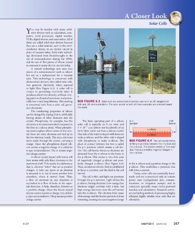
A B
ing parts or chemical reactions, and poten-
tially has a very long lifetime. This reading BOX FIGURE 6.3 Solar cells are economical in remote uses such as (A) navigational
is concerned with how a solar cell gener- aids and (B) communications. The solar panels in both of these examples are oriented toward
ates electricity. the south.
The conducting properties of silicon
can be changed by doping, that is, artificially
forcing atoms of other elements into the
crystal. Phosphorus, for example, has five The basic operating part of a silicon
electrons in its outermost shell compared to solar cell is typically an 8 cm wide and
−1
the four in a silicon atom. When phospho- 3 × 10 mm (about one-hundredth of an
rus atoms replace silicon atoms in the crys- inch) thick wafer cut from a silicon crystal.
tal, there are extra electrons not tied up in One side of the wafer is doped with boron to
the two electron bonds. The extra electrons make p-silicon, and the other side is doped
move easily through the crystal, carrying a with phosphorus to make n-silicon. The BOX FIGURE 6.4 The cell barrier forms
charge. Since the phosphorus-doped sili- place of contact between the two is called at the p-n junction between the n-silicon and
con carries a neg ative charge, it is called an the p-n junction, which creates a cell bar- the p-silicon. The barrier creates a “one-way”
n-type semiconductor. The n means nega- rier. The cell barrier forms as electrons are door that accumulates negative charges in
tive charge carrier. attracted from the n-silicon to the holes in the n-silicon.
A silicon crystal doped with boron will the p-silicon. This creates a very thin zone
have atoms with only three electrons in the of negatively charged p-silicon and posi-
outermost shell. This results in a deficiency, tively charged n-silicon (Box Figure 6.4). in the n-silicon and a positive charge in the
that is, electron “holes” that act as positive Thus, an internal electric field is established p-silicon. This establishes a potential that
charges. A hole can move as an electron at the p-n junction, and the field is the cell will drive a current.
is attracted to it, but it leaves another hole barrier. Today, solar cells are essentially hand-
elsewhere, where it moved from. Thus, The cell is thin, and light can penetrate made and are economical only in remote
a flow of electrons in one direction is through the p-n junction. Light strikes the power uses (navigational aids, commu-
equivalent to a flow of holes in the oppo- p-silicon, freeing electrons. Low-energy free nications, or irrigation pumps) and in
site direction. A hole, therefore, behaves as electrons might combine with a hole, but consumer specialty items (solar-powered
a positive charge. Since the boron-doped high-energy electrons cross the cell barrier watches and calculators). Research contin-
silicon carries a positive charge, it is called a into the n-silicon. The electron loses some ues on finding methods of producing highly
p-type semiconductor. The p means positive of its energy, and the barrier prevents it from efficient, highly reliable solar cells that are
charge carrier. returning, creating an excess negative charge affordable.
6-29 CHAPTER 6 Electricity 167