Page 68 - Digital Electronics by harish
P. 68

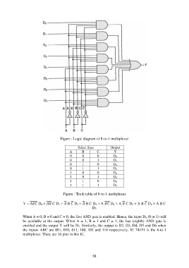
Figure : Logic diagram of 8-to-1 multiplexer

                                                  Select lines         Output
                                             A       B        C          Y
                                             0       0        0          D 0
                                             0       0        1          D 1
                                             0       1        0          D 2
                                             0       1        1          D 3
                                             1       0        0          D 4
                                             1       0        1          D 5
                                             1       1        0          D 6
                                             1       1        1          D 7

                                         Figure : Truth table of 8-to-1 multiplexer

                Y =  D 0 +  C D 1 +  B  D 2 +  B C D 3 + A  D 4 + A  C D 5 + A B  D 6 + A B C
                                                           D 7

               When A = 0, B = 0 and C = 0, the first AND gate is enabled. Hence, the input D 0 (0 or 1) will
               be available at  the output.  When A =  1, B = 1 and  C  = 1, the  last  (eighth)  AND  gate is
               enabled and the output Y will be D 7. Similarly, the output is D2, D3, D4, D5 and D6 when
               the inputs ABC are 001, 010, 011, 100, 101 and 110 respectively.  IC 74151  is  the 8-to-1
               multiplexer. There are 16 pins in this IC.


                                                           68
   63   64   65   66   67   68   69   70   71   72   73