
Page 72 - Digital Electronics by harish
P. 72
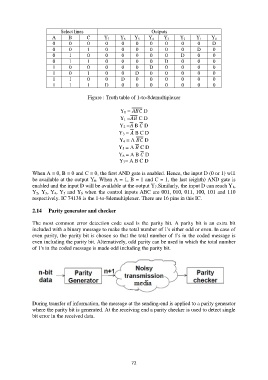
Select lines                            Outputs
                        A       B       C      Y 7     Y 6   Y 5   Y 4    Y 3    Y 2    Y 1    Y 0
                        0       0       0       0      0     0      0     0       0      0     D
                        0       0       1       0      0     0      0     0       0      D      0
                        0       1       0       0      0     0      0     0      D       0      0
                        0       1       1       0      0     0      0     D       0      0      0
                        1       0       0       0      0     0     D      0       0      0      0
                        1       0       1       0      0     D      0     0       0      0      0
                        1       1       0       0      D     0      0     0       0      0      0
                        1       1       1       D      0     0      0     0       0      0      0

                                        Figure : Truth table of 1-to-8demultiplexer

                                                      Y 0 =  D
                                                      Y 1 = C D
                                                      Y 2 = B  D
                                                      Y 3 =  B C D
                                                      Y 4 = A  D
                                                      Y 5 = A  C D
                                                      Y 6 = A B  D
                                                      Y 7= A B C D

               When A = 0, B = 0 and C = 0, the first AND gate is enabled. Hence, the input D (0 or 1) will
               be available at the output Y 0. When A = 1, B = 1 and C = 1, the last (eighth) AND gate is
               enabled and the input D will be available at the output Y 7.Similarly, the input D can reach Y 1,
               Y 2, Y 3, Y 4, Y 5 and Y 6 when the control inputs ABC are 001, 010, 011, 100, 101 and 110
               respectively. IC 74138 is the 1-to-8demultiplexer. There are 16 pins in this IC.

               2.14  Parity generator and checker

               The  most  common  error  detection  code  used  is  the  parity  bit.  A  parity  bit  is  an  extra  bit
               included with a binary message to make the total number of 1's either odd or even. In case of
               even parity, the parity bit is chosen so that the total number of 1's in the coded message is
               even including the parity bit. Alternatively, odd parity can be used in which the total number
               of 1's in the coded message is made odd including the parity bit.


               During transfer of information, the message at the sending-end is applied to a parity generator
               where the parity bit is generated. At the receiving end a parity checker is used to detect single
               bit error in the received data.


                                                           72