
Page 137 - Softcopy for Teachers buku kerja + nota Nilam Publications
P. 137
MODUL • Fizik TINGKATAN 5
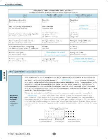
Perbandingan antara semikonduktor jenis-n dan jenis-p
The comparison between the n-type semiconductor and p-type semiconductor
Aspek Semikonduktor jenis-n Semikonduktor jenis-p
Aspect n-type semiconductor p-type semiconductor
Ketulenan semikonduktor Tidak tulen Tidak tulen
The purity of semiconductor Not pure Not pure
Jenis atom pendop yang digunakan Atom pentavalen Atom trivalen
The type of dopant atom used Pentavalent atom Trivalent atom
(i) fosforus / phosphorus (i) boron
Contoh-contoh atom pendop yang digunakan (ii) arsenik / arsenic (ii) indium
The examples of dopant atom used
(iii) antimoni / antimony (iii) gallium
Kesan ke atas kekonduksian elektrik Meningkat / menjadi lebih baik Meningkat / menjadi lebih baik
The effect on electrical conductivity Increases / becomes better Increases / becomes better
Bilangan elektron valens atom pendop 5 elektron 3 elektron
The number of valence electron of dopant atom 5 electrons 3 electrons
Pembawa cas majoriti Elektron bebas (cas negatif) Lohong (cas positif)
The majority charge carrier Free electrons (negatively charged) Holes (positively charged)
Pembawa cas minoriti Lohong (cas positif) Elektron bebas (cas negatif)
The minority charge carrier Holes (positively charged) Free electrons (negatively charged)
Diod semikonduktor / Semiconductor diodes
UNIT 4
• Apabila bahan semikonduktor jenis-p bercantum dengan bahan semikonduktor jenis-n, ini akan membentuk
UNIT 4
satu lapisan di tengah-tengahnya yang dinamakan lapisan susutan . Pada lapisan ini, elektron dari
bahan jenis-n hanyut merentasi simpang untuk mengisi lohong dalam bahan jenis-p. Lohong dari bahan jenis-p
menghanyut dalam arah bertentangan ke bahan jenis-n. Hasilnya, lapisan susutan yang nipis terbentuk. Ia
adalah kawasan sempit yang kehilangan semua elektron bebas dan lohong dan bersifat seperti silikon tulen
yang mempunyai kerintangan tinggi. Pengaliran cas seterusnya yang merentasi sempadan lapisan susutan akan
ditolak oleh cas di dalam lapisan tersebut.
When a p-type semiconductor material is in contact with an n-type semiconductor material, a layer called the
Bagaimana depletion layer is formed in the middle. At this junction, electrons from n-type semiconductor drifts
simpang p-n across the junction to fill in the holes in the p-type semiconductor. The holes from the p-type semiconductor drift
berfungsi? in the opposite direction to the n-type semiconductor. As a result, a depletion layer is produced. It is a very narrow
How the region which has lost all its available free electrons and holes and thus behaves almost like a pure silicon, with high
p-n junction resistivity. Any further movement of charges across the boundry in the depletion layer will be repelled by the charges
works? in the layer.
Voltan simpang / Junction voltage
Semikonduktor jenis-p Lapisan susutan Semikonduktor jenis-n
p-type semiconductor Depletion layer n-type semiconductor
© Nilam Publication Sdn. Bhd. 138