
Page 106 - Digital Electronics by harish
P. 106
Control signals:
In addition to the address and data lines, there are some control signals like Chip
Select (CS), Read (RD) and Write (WR). CS is used to select the memory chip, only when
CS is active (CS = 1), the RAM chip will work. WR line used while writing the data into the
memory locations and RD line is used while reading the data from the memory location
selected by the address inputs.
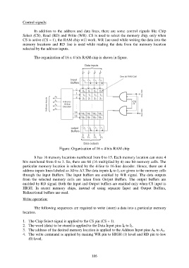
The organization of 16 x 4 bits RAM chip is shown in figure.
Figure: Organization of 16 x 4 bits RAM chip
It has 16 memory locations numbered from 0 to 15. Each memory location can store 4
bits numbered from 0 to 3. So, there are 64 (16 multiplied by 4) one bit memory cells. The
particular memory location is selected by the 4-line to 16-line decoder. Hence, there are 4
address inputs lines labeled as A0 to A3.The data inputs I 0 to I 3 are given to the memory cells
through the Input Buffers. The Input buffers are enabled by WR signal. The data outputs
from the selected memory cells are taken from Output Buffers. The output buffers are
enabled by RD signal. Both the Input and Output buffers are enabled only when CS input is
HIGH. In recent memory chips, instead of using separate Input and Output Buffers,
Bidirectional buffers are used.
Write operation:
The following sequences are required to write (store) a data into a particular memory
location.
1. The Chip Select signal is applied to the CS pin (CS = 1).
2. The word (data) to be stored is applied to the Data Input pins I 0 to I 3.
3. The address of the desired memory location is applied to the Address Input pins A 0 to A 3.
4. The write command is applied by making WR pin to HIGH (1) level and RD pin to low
(0) level.
106