
Page 101 - Digital Electronics by harish
P. 101
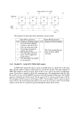
The sequence for input and output operations is given in table.

                               Input (Write) operation             Output (Read) operation
                         S.No  Sequence (Sequence Input)  S.No  Sequence (Parallel Output)
                                 Press the Master RESET
                           1.
                                 switch to clear all the FFs.
                                 Give the serial data to the
                           2.    Serial Input terminal SI,           The 4-bits parallel data are
                                 one by one (4 bits).         1.     taken out from ABCD
                                 For each input, one clock
                           3.    pulse must be applied (4            terminals.
                                 clock pulses).
                                 The data (4 bits) are stored
                           4.
                                 in the four FFs.

               3.3.4  Parallel IN – Serial OUT (PISO) Shift register

                       In PISO shift register the input is given in parallel form (i.e. all the bits at the same
               time) and the output is taken in serial form (i.e. one bit by one bit). The logic diagram of
               SIPO shift register is shown in figure. Four D FFs A, B, C and D are used is synchronous
               mode. Clock pulse is applied to all the FFs simultaneously. The Parallel Input data PI A, PI B,
               PI C and PI D are given to the PRESET terminals of the FFs through NAND gates. The NAND
               gates are enabled by the LOAD switch. The Q output of FF A is given to the D input of FF B.
               The Q output of FF B is given to the D input of FF C. The Q output of FF C is given to the D
               input of FF D. The Serial Output data (SO) is taken from the Q output of FF D. The CLEAR
               inputs of all the FFs are connected to ground through the Master Reset switch.


                                                           101