
Page 107 - Digital Electronics by harish
P. 107
Read operation:
The following sequences are required to read the data from a particular memory location.
1. The Chip Select signal is applied to the CS pin (CS = 1).
2. The address of the desired memory location is applied to the Address Input pins A 0 to A 3.
3. The read command is applied by making RD pin to HIGH (1) level and WR pin to low
(0) level.
4. Data will be available at the Data output pins O 1 to O 3.
4.3 Static RAM (SRAM)
RAM is classified into Static RAM and Dynamic RAM. Static RAM can retain the
data indefinite time as long as the power is present. But, in Dynamic RAM the stored data
will gradually disappear even when the power is present. Hence, we need to refresh the
Dynamic RAM periodically.
Static RAM circuits can be constructed using Bipolar Junction Transistor (BJT) or
Metal Oxide Semiconductor Field Effect Transistor (MOSFET). Based on the type of
transistor used, SRAM is classified into:
1. Bipolar Static RAM
2. MOS Static RAM
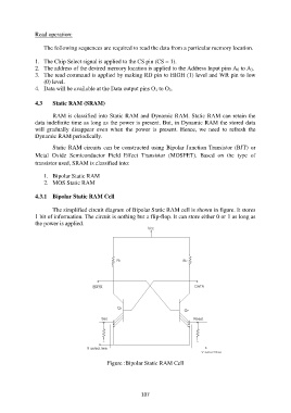
4.3.1 Bipolar Static RAM Cell
The simplified circuit diagram of Bipolar Static RAM cell is shown in figure. It stores
1 bit of information. The circuit is nothing but a flip-flop. It can store either 0 or 1 as long as
the power is applied.
Figure :Bipolar Static RAM Cell
107