
Page 80 - Digital Electronics by harish
P. 80
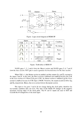
Figure : Logic circuit diagram of JKMS FF

                                    Inputs                   Outputs
                              CLK      J      K          Q                      Condition
                                                      Previous      Previous
                                       0      0                                   No change
                                                       value          value
                                       0      1          0              1           Reset


                                       1      0          1              0            Set

                                                    Complement  Complement
                                       1      1     of Previous    of Previous     Toggle
                                                       value          value


                                             Figure : Truth table of JKMS FF

                       NAND gates 1, 2, 3 and 4 form the Master section and NAND gates 5, 6, 7 and 8
               form the slave section. NOT gate is used to generate the inverted clock for the slave section.

                       When CLK = 1, the Master section in enabled and the outputs Q M and  M respond to
               the inputs J and K. At this time, the Slave section is inhibited (not enabled) because the CLK
               to the slave section is 0. When CLK goes LOW, the Master section is inhibited and the Slave
               section is enabled, because its CLK input is HIGH. Therefore, the outputs Q and  follow Q M
               and  M respectively. Hence, the slave section follows the master section.

                       The input to the gates 3 and 4 do not change during the clock pulse, therefore the
               race-around  condition  does  not  exist.  The  state  of  the  JKMS  FF  changes  at  the  negative
               transition  (trailing  edge)  of  the  clock  pulse.  The  Pr  and  Cr  inputs  are  used  to  SET  and
               CLEAR the FF irrespective of the clock input.


                                                           80