
Page 76 - Digital Electronics by harish
P. 76
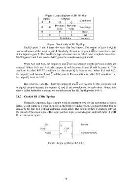
Figure : Logic diagram of SR flip-flop
                                        Inputs          Outputs
                                      S      R        Q                Condition
                                                   Previous  Previous
                                       0     0                           No change
                                                    value      value
                                       0     1        0          1         Reset
                                       1     0        1          0          Set
                                       1     1         Forbidden          Not used

                                            Figure : Truth table of SR flip-flop
                       NAND  gates  3  and  4  form  the  basic  flip-flop  circuit.  The  output  of  gate  3  (Q)  is
               connected as one of the input to gate 4. Similarly, the output of gate 4 () is connected as one
               of the input to gate 3. This feedback type of connection is called cross coupled connection.
               NAND gates 1 and 2 are used as NOT gates for complementing S and R.

                       When S=1 and R=1, the outputs Q and  will not change and the previous values are
               retained.  When  S=0  and  R=1,  the  output  Q  will  become  0  and    will  become  1.  This
               condition is called RESET condition. i.e. the output Q is reset to zero. When S=1 and R=0,
               the output Q will become 1 and  will become 0. This condition is called SET condition. i.e.
               the output Q is set to ONE.

                       But, when S=1 and R=1, both the outputs Q and  will become 1. This is not allowed
               in digital circuits because the outputs Q and   are complement to each other. Hence, this
               state is called forbidden state and we should not use the SR flip-flop with S=R=1.

               3.1.2  Clocked SR (CSR) flip-flop

                       Normally, sequential logic circuits work in sequence with on the occurrence of clock
               signal. Clock signal is a train of pulses in the form of square wave. Clocked SR flip-flop is
               similar to SR flip-flop with an additional clock input. The output of the FF changes only on
               the arrival of the clock signal. The logic symbol, logic circuit diagram and truth table of CSR
               FF are shown in figure.


                                            Figure : Logic symbol of CSR FF


                                                           76