
Page 89 - Digital Electronics by harish
P. 89
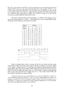
flip-flop A. The Q output of the FF A is given as clock input to the second flip-flop B. The Q
               output of FF B is given as clock input to the third flip-flop C. The Q output of FF C is given
               as clock input to the fourth flip-flop D. The Q output of all the flip-flops are taken as the
               counter outputs DCBA. The output A is called the Least Significant Bit LSB) and the output
               D  is  called  the  Most  Significant  Bit  (MSB).  The  CLEAR  (Cr)  input  of  all  the  FFs  are
               connected to ground through the Master Reset switch.

                                                        th
                       We need to reset the counter at 10  clock pulse i.e. at DCBA = 1010. Hence, we have
               to reset the counter when D = 1 and B = 1. The NAND gate is used to apply RESET signal.
               The inputs for the NAND gate are taken from D and B.


                                            Input            Output
                                            Clock    D       C     B      A
                                            Reset     0      0      0     0
                                              1       0      0      0     1
                                              2       0      0      1     0
                                              3       0      0      1     1
                                              4       0      1      0     0
                                              5       0      1      0     1
                                              6       0      1      1     0
                                              7       0      1      1     1
                                              8       1      0      0     0
                                              9       1      0      0     1
                                             10       0      0      0     0
                                             11       0      0      0     1


                       When  the  Master  Reset  switch  is  pressed,  all  the  FFs  are  cleared  and  the  counter
               output DCBA is 0000. During the negative edge of the first clock pulse, FF A will be toggled
               i.e. the output A changes from 0 to 1. At this time, the outputs of all other flip-flops will not
               change. Hence, the counter output DCBA is 0001. During the application of the second clock
               pulse, FF A will be toggled once again from 1 to 0. This will give a negative edge triggering
               pulse  to  FF  B  and  hence  FF  B  also  toggles  from  0  to  1.  The  counter  output  DCBA  will
               become 0010. Similarly the counting continues.

                                th
                       At the 10  clock pulse, the output DCBA will try to become 1010 (D = 1 and B = 1).
               As the NAND gate inputs, D and B are 11, the 0 in the gate output RESET the counter. The
               frequency of output D is 1/10 of clock signal frequency. Hence, the mod-10 counter acts as a
               „divided by 10‟ counter. The outputs of the counter during the application of each clock pulse
               are shown in the truth table and also in the waveforms.


                                                           89