
Page 94 - Digital Electronics by harish
P. 94
From the truth table we may observe that the output A toggles in every clock pulse,
output B toggles when output A is 1, output C toggles when both A and B are 1, output C
toggles when A, B and C are 1. This can be achieved by using AND gates as shown in the
figure. Toggle input of FF A is directly connected to +5v, hence, FF A toggles for every
clock pulse. The Q output of the FF A is connected to the Toggle input of FF B, hence, FF B
toggles only when A is 0. The output of AND gate 1, whose inputs are A and B, is connected
to the Toggle input of FF C, hence, FF C toggles only when Aand B are 1. Similarly, the
output of AND gate 2, whose inputs are the output of AND gate 1 and C, is connected to the
Toggle input of FF D, hence, FF D toggles only when A, B and C are 1.
The frequency of output A is ½ of the clock frequency, output B is ¼ of clock, output
C is 1/8 of clock and output D is 1/16 of clock frequency. Hence, the four bit counter acts as a
th
th
„divided by 16‟ counter.For the 15 clock pulse, the output is 1111. When the next (16 )
clock pulse is applied, all the flip-flops will toggle from 1 to 0 at the same time and hence the
output is 0000. The outputs of the counter during the application of each clock pulse are
shown in the waveforms.
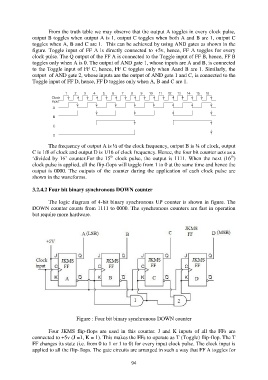
3.2.4.2 Four bit binary synchronous DOWN counter
The logic diagram of 4-bit binary synchronous UP counter is shown in figure. The
DOWN counter counts from 1111 to 0000. The synchronous counters are fast in operation
but require more hardware.
Figure : Four bit binary synchronous DOWN counter
Four JKMS flip-flops are used in this counter. J and K inputs of all the FFs are
connected to +5v (J =1, K = 1). This makes the FFs to operate as T (Toggle) flip-flop. The T
FF changes its state (i.e. from 0 to 1 or 1 to 0) for every input clock pulse. The clock input is
applied to all the flip-flops. The gate circuits are arranged in such a way that FF A toggles for
94