
Page 92 - Digital Electronics by harish
P. 92
LSB) and the output C is called the Most Significant Bit (MSB). The CLEAR (Cr) input of
all the FFs are connected to ground through the Master Reset switch.
th
We need to reset the counter at 7 clock pulse i.e. at CBA = 111. Hence, we have to
reset the counter when C = 1, B = 1 and A = 1. The NAND gate is used to apply RESET
signal. The inputs for the NAND gate are taken from C, B and A.
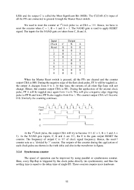
Input Output
Clock C B A
Reset 0 0 0
1 0 0 1
2 0 1 0
3 0 1 1
4 1 0 0
5 1 0 1
6 1 1 0
7 0 0 0
8 0 0 1
When the Master Reset switch is pressed, all the FFs are cleared and the counter
output CBA is 000. During the negative edge of the first clock pulse, FF A will be toggled i.e.
the output A changes from 0 to 1. At this time, the outputs of all other flip-flops will not
change. Hence, the counter output CBA is 001. During the application of the second clock
pulse, FF A will be toggled once again from 1 to 0. This will give a negative edge triggering
pulse to FF B and hence FF B also toggles from 0 to 1. The counter output CBA will become
010. Similarly the counting continues.
th
At the 7 clock pulse, the output CBA will try to become 111 (C = 1, B = 1 and A =
1). As the NAND gate inputs, C, B and A are 111, the 0 in the gate output RESET the
counter. The frequency of output C is 1/7 of clock signal frequency. Hence, the mod-7
counter acts as a „divided by 7‟ counter. The outputs of the counter during the application of
each clock pulse are shown in the truth table and also in the waveforms in figure.
3.2.4 Synchronous counter
The speed of operation can be improved by using parallel or synchronous counter.
Here, every flip-flop is triggered by the clock pulse directly (in synchronism), and thus the
settling time is equal to the delay time of single FF. These counters require more hardware.
92