
Page 91 - Digital Electronics by harish
P. 91
When the Master Reset switch is pressed, all the FFs are cleared and the counter
output BA is 00. During the negative edge of the first clock pulse, FF A will be toggled i.e.
the output A changes from 0 to 1. At this time, the outputs of all other flip-flops will not
change. Hence, the counter output BA is 01. During the application of the second clock pulse,
FF A will be toggled once again from 1 to 0. This will give a negative edge triggering pulse
to FF B and hence FF B also toggles from 0 to 1. The counter output BA will become 10.
rd
At the 3 clock pulse, the output BA will try to become 11 (B = 1 and A = 1). As the
NAND gate inputs, B and A are 11, the 0 in the gate output RESET the counter. The
frequency of output B is 1/3 of clock signal frequency. Hence, the mod-3 counter acts as a
„divided by 3‟ counter. The outputs of the counter during the application of each clock pulse
are shown in the truth table and also in the waveforms.
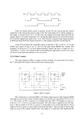
3.2.3.2 Mod-7 counter
The logic diagram of Mod-7 counter is shown in figure. It counts from 0 to 6 and at
th
the 7 clock pulse the counter will reset and starts counting again.
Figure : Mod-7 counter
The counter has to count from 000 to 110. Hence, three negative edge triggered JKMS
flip-flops are used in this counter. J and K inputs of all the FFs are connected to +5v (J =1, K
= 1). This makes the FFs to operate as T (Toggle) flip-flop. The T FF changes its state (i.e.
from 0 to 1 or 1 to 0) for every input clock pulse. The clock input is applied to the first flip-
flop A. The Q output of the FF A is given as clock input to the second flip-flop B. The Q
output of FF B is given as clock input to the third flip-flop C. The Q output of all the flip-
flops are taken as the counter outputs CBA. The output A is called the Least Significant Bit
91