
Page 95 - Digital Electronics by harish
P. 95
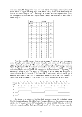
every clock pulse, FF B toggles for every two clock pulses, FF C toggles for every four clock
               pulses and FF D toggles for every eight clock pulses. The Q output of all the flip-flops are
               taken as the counter outputs ABCD. The output A is called the Least Significant Bit (LSB)
               and the output D is called the Most Significant Bit (MSB). The truth table of the counter is
               shown in figure.

                                            Input            Output
                                            Clock    D       C     B      A
                                            Reset     0      0      0     0
                                              1       1      1      1     1
                                              2       1      1      1     0
                                              3       1      1      0     1
                                              4       1      1      0     0
                                              5       1      0      1     1
                                              6       1      0      1     0
                                              7       1      0      0     1
                                              8       1      0      0     0
                                              9       0      1      1     1
                                             10       0      1      1     0
                                             11       0      1      0     1
                                             12       0      1      0     0
                                             13       0      0      1     1
                                             14       0      0      1     0
                                             15       0      0      0     1
                                             16       0      0      0     0

                       From the truth table we may observe that the output A toggles in every clock pulse,
               output B toggles when output A is 0, output C toggles when both A and B are 0, output C
               toggles when A, B and C are 0.  This can be achieved by using AND gates as shown in the
               figure. Toggle input of FF A is  directly connected to  +5v, hence, FF A toggles for every
               clock pulse. The  A output of the FF A is connected to the Toggle input of FF B, hence, FF B
               toggles  only  when  A  is  0.  The  output  of  AND  gate  1,  whose  inputs  are   A  and B,  is
               connected  to  the  Toggle  input  of  FF  C,  hence,  FF  C  toggles  only  when  A  and  B  are  0.
               Similarly, the output  of AND gate 2, whose inputs are the output of AND gate 1 and  C, is
               connected to the Toggle input of FF D, hence, FF D toggles only when A, B and C are 0.


                       The frequency of output A is ½ of the clock frequency, output B is ¼ of clock, output
               C is 1/8 of clock and output D is 1/16 of clock frequency. Hence, the four bit counter acts as a
                                                  th
                                                                                                        th
               „divided by 16‟ counter.For the 15  clock pulse, the output is 0000. When the next (16 )
               clock pulse is applied, all the flip-flops will toggle from 0 to 1 at the same time and hence the


                                                           95